- 您现在的位置:买卖IC网 > Sheet目录250 > SFCF2048H1BO2TO-I-M0-523-SMA (Swissbit NA Inc)FLASH SLC UDMA/MDMA/PIO 2G
�� �
�
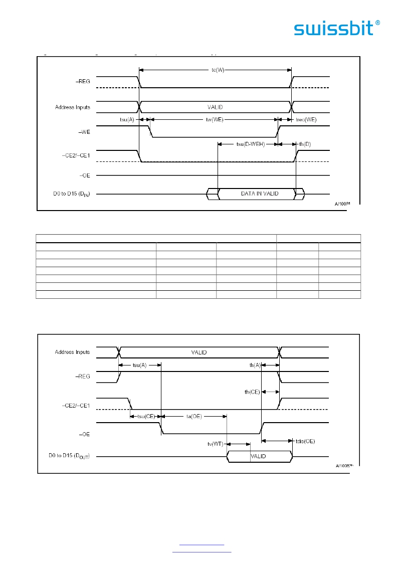
�Figure� 3:� Configuration� Register� (Attribute� Memory)� Write� waveforms�
�16�
�D� IN� signifies� data� provided� by� the� system� to� the� CompactFlash� Card.�
�Table� 19:� Configuration� Register� (Attribute� Memory)� Write� timing�
�Speed� Version�
�250ns�
�Item�
�Write� Cycle� Time�
�Write� Pulse� Width�
�Address� Setup� Time�
�Data� Setup� Time� for� WE�
�Data� Hold� Time�
�Write� Recovery� Time�
�Symbol�
�tc(W)�
�tw(WE)�
�tsu(A)�
�tsu(D-WEH)�
�th(D)�
�trec(WE)�
�IEEEE� Symbol�
�tAVAV�
�tWLWH�
�tAVWL�
�tDVWH�
�tWMDX�
�tWMAX�
�Min.� (ns)�
�250�
�150�
�30�
�80�
�30�
�30�
�Max.� (ns)�
�6.2� Common� Memory� Read� and� Write�
�Figure� 4:� Common� Memory� Read� waveforms�
�17�
�D� OUT� means� data� provided� by� the� CompactFlash� Memory� Card� to� the� system.�
�Swissbit� AG�
�Industriestrasse� 4�
�Swissbit� reserves� the� right� to� change� products� or� specifications� without� notice.�
�Revision:� 1.20�
�CH-9552� Bronschhofen�
�Switzerland�
�www.swissbit.com�
�industrial@swissbit.com�
�C-320_data_sheet_CF-HxBO_Rev120.doc�
�Page� 19� of� 101�
�发布紧急采购,3分钟左右您将得到回复。
相关PDF资料
SFCF4096H4BK2SA-I-QT-553-SMA
FLASH SLC UDMA/MDMA/PIO 4G
SFCF64GBH2BU4TO-I-NU-517-STD
FLASH SLC UDMA/MDMA/PIO 64GB
SFN08B4702CBQLF7
RES ARRAY 47K OHM 7 RES 8-DFN
SFP1050-12BG
FRONT END AC/DC 1050W 12V
SFP450-12BG
PWR SUP 450W 12V 36.6A W/STANDBY
SFSD1024N1BN1TO-I-DF-151-STD
FLASH MICRO SD CARD IND S-200 1G
SFSD2048L1BN2TO-I-DF-151-STD
FLASH SECURE DGTL CARD SD 2G
SFSD4096L1BN2TO-I-Q2-141-STD
FLASH SECURE DGTL CARD SDHC 4G
相关代理商/技术参数
SFCF2048H1BO2TO-I-M0-533-ZP1
制造商:SWISSBIT NA INC 功能描述:FLASH
SFCF2048H1BO2TO-I-M0-543-SMA
制造商:SWISSBIT NA INC 功能描述:FLASH
SFCF2048H2BU2TO-C-MS-527-STD
制造商:SWISSBIT NA INC 功能描述:FLASH
SFCF2048H2BU2TO-I-MS-517-STD
功能描述:FLASH SLC UDMA/MDMA/PIO 2GB RoHS:是 类别:存储卡,模块 >> 存储器,PC 卡 系列:C-440 标准包装:30 系列:- 存储容量:8GB 存储器类型:存储卡 - Extreme III SD?
SFCF2048H2BU2TO-I-MS-527-STD
制造商:SWISSBIT NA INC 功能描述:FLASH
SFCF2048H4BK1SA-C-QT-553-SMA
制造商:SWISSBIT NA INC 功能描述:FLASH
SFCF2048H4BK1SA-I-QT-553-SMA
功能描述:FLASH SLC UDMA/MDMA/PIO 2G RoHS:是 类别:存储卡,模块 >> 存储器,PC 卡 系列:C-300 标准包装:30 系列:- 存储容量:8GB 存储器类型:存储卡 - Extreme III SD?
SFCF2048H4BK2SA-C-DS-553-SMA
制造商:SWISSBIT NA INC 功能描述:FLASH SLC UDMA/MDMA/PIO 2G